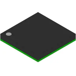
Las imágenes son solo para referencia
XCKU15P-L2FFVA1156E
IC FPGA 516 I/O 1156FCBGA
- Fabricante
- Mfr. Parte #XCKU15P-L2FFVA1156E
- Paquete FCBGA-1156
- Hoja de datos
- En stock5743
100% original & Nuevo
24 horas listos para el envío
Garantía de 365 días
RFQ y Obtenga más descuentos
Especificaciones
| Package | Tray |
| Series | Kintex® UltraScale+™ |
| ProductStatus | Active |
| NumberofLABs/CLBs | 65340 |
| NumberofLogicElements/Cells | 1143450 |
| TotalRAMBits | 82329600 |
| NumberofI/O | 516 |
| Voltage-Supply | 0.698V ~ 0.876V |
| MountingType | Surface Mount |
| OperatingTemperature | 0°C ~ 100°C (TJ) |
| Package/Case | 1156-BBGA, FCBGA |
Descripción general
Description
The "L2" designation indicates a specific logic and routing architecture optimized for low power consumption while maintaining performance. The "FFVA1156E" package refers to its physical form factor, which supports efficient thermal management and integration into various systems.
Due to its capabilities, the XCKU15P is widely used in industries such as telecommunications, automotive, aerospace, and military, enabling rapid prototyping and deployment of advanced technologies. Its programmable nature allows for customization to meet specific application requirements, ensuring versatility and future-proofing in rapidly evolving markets.
Features
1. Logic Cells: Approximately 15,000 logic cells for complex digital designs.
2. DSP Slices: Contains 30 DSP slices optimized for high-speed arithmetic operations.
3. Memory: Includes multiple Block RAMs (BRAM) and UltraRAM for efficient data storage.
4. I/O: Supports a variety of high-speed serial interfaces, including PCIe Gen3 and high-speed transceivers (up to 6.6 Gbps).
5. Power Efficiency: Designed for low power consumption, making it suitable for power-sensitive applications.
6. Configuration: Flexible configuration options for various application needs, including partial reconfiguration.
7. Development Tools: Compatible with Xilinx development environments like Vivado, enabling efficient design and implementation.
This FPGA is ideal for applications in telecommunications, automotive, aerospace, and industrial sectors, where performance and flexibility are critical.
Package
Pinout
- Configurable I/O standards (e.g., LVDS, LVCMOS)
- High-speed serial transceivers
- Multiple configurable logic blocks
- DSP slices and memory resources
These functionalities make it suitable for a variety of applications, including data processing, high-speed networking, and signal processing. The device supports advanced power management and can be used in various industrial, telecommunications, and automotive applications.
Manufacturer
Application
Equivalent
Envío
Métodos de envíoNosotros
ofrecer servicios de envío globales a través de DHL, FedEx, TNT, UPS, o cualquier otro expediente de su elección.
Referencia de tarifas de envío (DHL/FedEx):
DHL: El costo de envío oscila entre $25-$45 (0.5kg), con un tiempo de entrega estimado de 2-5 días hábiles.
FedEx: El costo de envío oscila entre $25-$40 (0.5kg), con un tiempo de entrega estimado de 3-7 días hábiles.
UPS: El costo de envío oscila entre $25-$45 (0.5kg), con un tiempo de entrega estimado de 3-7 días hábiles.
TNT: El costo de envío oscila entre $25-$65 (0.5kg), con un tiempo de entrega estimado de 3-7 días hábiles.
EMS: El costo de envío oscila entre $30-$50 (0.5kg), con un plazo de entrega estimado de 7-15 días hábiles.
Correo aéreo registrado: El costo de envío es de $2-$4 (0.1kg), con un tiempo de entrega estimado de 5-20 días hábiles.
Pagos
Payment Methods
El plazo de pago es 100% prepagado.
Actualmente, solo aceptamos los siguientes métodos de pago:
1. de PayPal
2. Tarjeta de crédito/débito
3. Transferencia bancaria
Similar
-
![MX66U1G45GXDI00]() MX66U1G45GXDI00
Macronix
-
![MX25L8035EM2I-10G]() MX25L8035EM2I-10G
Macronix
-
![MX25L25673GMI-10G]() MX25L25673GMI-10G
Macronix
-
![MX29GL512FHXFI-11G]() MX29GL512FHXFI-11..
Macronix
-
![MX25U51279GXDR00]() MX25U51279GXDR00
Macronix
-
![MX25R1635FZUIH0]() MX25R1635FZUIH0
Macronix
-
![MX25V1635FM2I]() MX25V1635FM2I
Macronix
-
![MX25U3232FZBI02]() MX25U3232FZBI02
Macronix
-
![MX25L6433FM2I-08G]() MX25L6433FM2I-08G
Macronix
-
![MX25L12833FZ2I-10G]() MX25L12833FZ2I-10..
Macronix
-
![MX25L12833FZNI-10G]() MX25L12833FZNI-10..
Macronix
-
![MX29F040CQI-70G]() MX29F040CQI-70G
Macronix