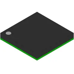
Las imágenes son solo para referencia
TLIN10283DRBRQ1
IC TRANSCEIVER 1/1 8VSON
- Fabricante
- Mfr. Parte #TLIN10283DRBRQ1
- Paquete VSON (DRB)-8
- Hoja de datos TLIN10283DRBRQ1 DataSheet
- En stock3128
100% original & Nuevo
24 horas listos para el envío
Garantía de 365 días
RFQ y Obtenga más descuentos
Especificaciones
| Package | Tape & Reel (TR),Cut Tape (CT) |
| Series | Automotive, AEC-Q100 |
| ProductStatus | Active |
| Type | Transceiver |
| Protocol | LIN |
| NumberofDrivers/Receivers | 1/1 |
| ReceiverHysteresis | 500 mV |
| DataRate | 100kbps |
| Voltage-Supply | 5.5V ~ 28V |
| OperatingTemperature | -40°C ~ 125°C |
| MountingType | Surface Mount, Wettable Flank |
| Package/Case | 8-VDFN Exposed Pad |
Descripción general
Description
Features
1. Voltage Monitoring: It offers precise monitoring of supply voltages, ensuring system reliability by detecting under-voltage conditions.
2. Multiple Threshold Options: The device supports various voltage thresholds, allowing customization based on specific application requirements.
3. Reset Output: It provides an active-low reset output that indicates when the monitored voltage is below the set threshold.
4. Wide Supply Voltage Range: Operates over a broad input voltage range, enhancing compatibility with diverse automotive electrical systems.
5. Low Quiescent Current: Ensures minimal power consumption, making it suitable for battery-operated devices.
6. Automotive Qualification: Designed to meet AEC-Q100 standards, ensuring robustness in harsh automotive environments.
7. Temperature Range: Supports operation over an extended temperature range, ensuring reliability in varying conditions.
These features make the TLIN10283DRBRQ1 ideal for automotive safety and control applications.
Package
Pinout
The functions of its pins are as follows:
1. VCC (Pin 1): Supply voltage for the device.
2. GND (Pin 2): Ground reference.
3. RX (Pin 3): LIN receive data input.
4. TX (Pin 4): LIN transmit data output.
5. RSON (Pin 5): Resistor for controlling the slope of the LIN signal.
6. VIO (Pin 6): Voltage supply for the logic interface.
7. SLEEP (Pin 7): Sleep mode control input.
8. LIN (Pin 8): LIN bus connection.
This device is optimized for low-power operation and provides robust data transfer on LIN networks.
Manufacturer
Application
Equivalent
Envío
Métodos de envíoNosotros
ofrecer servicios de envío globales a través de DHL, FedEx, TNT, UPS, o cualquier otro expediente de su elección.
Referencia de tarifas de envío (DHL/FedEx):
DHL: El costo de envío oscila entre $25-$45 (0.5kg), con un tiempo de entrega estimado de 2-5 días hábiles.
FedEx: El costo de envío oscila entre $25-$40 (0.5kg), con un tiempo de entrega estimado de 3-7 días hábiles.
UPS: El costo de envío oscila entre $25-$45 (0.5kg), con un tiempo de entrega estimado de 3-7 días hábiles.
TNT: El costo de envío oscila entre $25-$65 (0.5kg), con un tiempo de entrega estimado de 3-7 días hábiles.
EMS: El costo de envío oscila entre $30-$50 (0.5kg), con un plazo de entrega estimado de 7-15 días hábiles.
Correo aéreo registrado: El costo de envío es de $2-$4 (0.1kg), con un tiempo de entrega estimado de 5-20 días hábiles.
Pagos
Payment Methods
El plazo de pago es 100% prepagado.
Actualmente, solo aceptamos los siguientes métodos de pago:
1. de PayPal
2. Tarjeta de crédito/débito
3. Transferencia bancaria
Similar
-
![MX25R8035FM1IL0]() MX25R8035FM1IL0
Macronix
-
![MX25L3233FM1I-08Q]() MX25L3233FM1I-08Q
Macronix
-
![MX25V5126FM1I]() MX25V5126FM1I
Macronix
-
![MX25V4035FZUI]() MX25V4035FZUI
Macronix
-
![MX25V2033FM1I]() MX25V2033FM1I
Macronix
-
![MX25R3235FZNIL0]() MX25R3235FZNIL0
Macronix
-
![MX25V16066M2I02]() MX25V16066M2I02
Macronix
-
![MX25R6435FBDIL0]() MX25R6435FBDIL0
Macronix
-
![MX29GL512FHXFI-11G]() MX29GL512FHXFI-11..
Macronix
-
![MX25L6433FM2I-08G]() MX25L6433FM2I-08G
Macronix
-
![MX29LV160DTTI-70G]() MX29LV160DTTI-70G
Macronix
-
![MX29F800CBTI-70G]() MX29F800CBTI-70G
Macronix