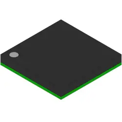
Las imágenes son solo para referencia
TC7WH125FU
- Fabricante
- Mfr. Parte #TC7WH125FU
- Paquete
- Hoja de datos
- En stock8963
100% original & Nuevo
24 horas listos para el envío
Garantía de 365 días
RFQ y Obtenga más descuentos
Especificaciones
| Brand | Toshiba |
| Subcategory | Logic ICs |
| Product Type | Buffers & Line Drivers |
| Series | TC7WH125 |
| Logic Family | WH |
Descripción general
Description
Key features of the TC7WH125FU include its ability to provide two independent buffers with three-state outputs, which can drive up to 15 LSTTL (Low-power Schottky TTL) loads. This attribute is essential for applications requiring data line isolation and multiplexing. The device also includes over-voltage tolerant inputs, allowing for interface compatibility with 5V logic when operating at lower voltages.
Packaged in a small, surface-mount TSSOP (Thin Shrink Small Outline Package), the TC7WH125FU is suitable for compact circuit designs. Its low power dissipation and high-speed operation make it ideal for use in personal electronics, computing, and communication devices where efficient signal management is crucial.
Features
1. Logic Type: Dual buffer.
2. Input Type: CMOS, which offers high noise immunity and low static power consumption.
3. Output Type: Push-pull.
4. Voltage Range: Operates over a range of voltages, typically around 2V to 6V.
5. Temperature Range: Suitable for standard commercial operating temperatures.
6. Package: Available in small surface-mount packages like USV (SOT-353).
7. Propagation Delay: Fast switching speeds, contributing to efficient signal processing.
8. Power Consumption: Low power consumption due to CMOS technology, making it suitable for battery-powered applications.
This component is ideal for applications requiring signal buffering and enhancing driving capability without altering the signal integrity.
Package
Pinout
Regarding its pin count and function:
- Pin Count: The TC7WH125FU is housed in an 8-pin package.
- Function: It includes two independent buffer/drivers. Each buffer/driver has an input, an output, and an output enable pin. When the output enable pin is low, the corresponding output is disabled (high-impedance state), allowing for shared bus applications. When the output enable pin is high, the input signal is propagated to the output, providing a strong drive capability.
This functionality is useful for controlling data flow and isolating different parts of a circuit, ensuring that signals are transmitted accurately and efficiently while preventing possible contention on shared bus lines.
Manufacturer
Application
Equivalent
Envío
Métodos de envíoNosotros
ofrecer servicios de envío globales a través de DHL, FedEx, TNT, UPS, o cualquier otro expediente de su elección.
Referencia de tarifas de envío (DHL/FedEx):
DHL: El costo de envío oscila entre $25-$45 (0.5kg), con un tiempo de entrega estimado de 2-5 días hábiles.
FedEx: El costo de envío oscila entre $25-$40 (0.5kg), con un tiempo de entrega estimado de 3-7 días hábiles.
UPS: El costo de envío oscila entre $25-$45 (0.5kg), con un tiempo de entrega estimado de 3-7 días hábiles.
TNT: El costo de envío oscila entre $25-$65 (0.5kg), con un tiempo de entrega estimado de 3-7 días hábiles.
EMS: El costo de envío oscila entre $30-$50 (0.5kg), con un plazo de entrega estimado de 7-15 días hábiles.
Correo aéreo registrado: El costo de envío es de $2-$4 (0.1kg), con un tiempo de entrega estimado de 5-20 días hábiles.
Pagos
Payment Methods
El plazo de pago es 100% prepagado.
Actualmente, solo aceptamos los siguientes métodos de pago:
1. de PayPal
2. Tarjeta de crédito/débito
3. Transferencia bancaria
Similar
-
![MX25L3233FM1I-08Q]() MX25L3233FM1I-08Q
Macronix
-
![MX25V1635FZNI]() MX25V1635FZNI
Macronix
-
![MX25R3235FZNIL0]() MX25R3235FZNIL0
Macronix
-
![MX25R6435FBDIL0]() MX25R6435FBDIL0
Macronix
-
![MX25L25673GMI-08G]() MX25L25673GMI-08G
Macronix
-
![MX25L25673GMI-10G]() MX25L25673GMI-10G
Macronix
-
![MX29GL512FHXFI-11G]() MX29GL512FHXFI-11..
Macronix
-
![MX25U51279GXDR00]() MX25U51279GXDR00
Macronix
-
![MX25U25643GZNI00]() MX25U25643GZNI00
Macronix
-
![MX25U6435FM2I-10G]() MX25U6435FM2I-10G
Macronix
-
![MX25L12833FM2I-10G]() MX25L12833FM2I-10..
Macronix
-
![MX25U25645GXDI00]() MX25U25645GXDI00
Macronix