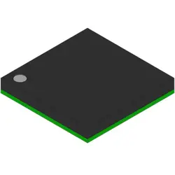
Las imágenes son solo para referencia
TC7S04FU
Inverters
- Fabricante
- Mfr. Parte #TC7S04FU
- Paquete
- Hoja de datos TC7S04FU DataSheet
- En stock7644
100% original & Nuevo
24 horas listos para el envío
Garantía de 365 días
RFQ y Obtenga más descuentos
Especificaciones
| Standard Pack Qty | 10000 |
Descripción general
Description
The TC7S04FU is characterized by low power consumption and high-speed performance, with fast switching times, which is ideal for enhancing signal integrity in digital circuits. It is often utilized in applications such as signal conditioning, interfacing, and logic level shifting.
In terms of packaging, the TC7S04FU comes in a compact form factor, making it suitable for space-constrained designs. The device also offers a high noise margin and a wide input voltage range, ensuring reliable operation in various environments. Overall, the TC7S04FU is a robust choice for designers looking for efficient and reliable logic inversion in their electronic projects.
Features
1. Voltage Range: Operates within a power supply range of 2.0V to 5.5V.
2. High Speed: Offers fast switching times, typically around 10 ns at 5V, making it suitable for high-speed applications.
3. Low Power Consumption: Designed for low static and dynamic power consumption, enhancing energy efficiency.
4. High Noise Immunity: Features a high noise margin, ensuring reliable operation in noisy environments.
5. Wide Operating Temperature: Suitable for a temperature range of -40°C to 125°C, allowing flexibility in various applications.
6. Compact Package: Available in a small footprint package, such as the SSOP or TSSOP, beneficial for space-constrained designs.
7. Multiple Functionality: Each of the six buffers can independently invert its input signal, providing versatile logic solutions.
These features make the TC7S04FU suitable for a variety of digital logic applications in consumer electronics, automotive, and industrial devices.
Package
Pinout
Pin Functions:
1. Inputs (A1 to A6): Pins 1, 2, 3, 5, 6, and 9 serve as the inputs for the six inverter gates.
2. Outputs (Y1 to Y6): Pins 4, 10, 11, 12, 13, and 14 are the corresponding outputs for each inverter gate.
3. VCC (Pin 7): Power supply pin, typically connected to +3V to +5.5V.
4. GND (Pin 8): Ground pin, connected to 0V.
The TC7S04FU operates at low power and provides fast switching speeds, making it suitable for various digital logic applications.
Manufacturer
Application
Equivalent
1. 74LVC20A (Low Voltage CMOS)
2. 74HC20 (High-Speed CMOS)
3. 74HCT20 (TTL-compatible)
4. CD4011 (Dual 2-input NAND, but may differ in configuration)
Always check specific datasheets for pin compatibility and electrical characteristics.
Envío
Métodos de envíoNosotros
ofrecer servicios de envío globales a través de DHL, FedEx, TNT, UPS, o cualquier otro expediente de su elección.
Referencia de tarifas de envío (DHL/FedEx):
DHL: El costo de envío oscila entre $25-$45 (0.5kg), con un tiempo de entrega estimado de 2-5 días hábiles.
FedEx: El costo de envío oscila entre $25-$40 (0.5kg), con un tiempo de entrega estimado de 3-7 días hábiles.
UPS: El costo de envío oscila entre $25-$45 (0.5kg), con un tiempo de entrega estimado de 3-7 días hábiles.
TNT: El costo de envío oscila entre $25-$65 (0.5kg), con un tiempo de entrega estimado de 3-7 días hábiles.
EMS: El costo de envío oscila entre $30-$50 (0.5kg), con un plazo de entrega estimado de 7-15 días hábiles.
Correo aéreo registrado: El costo de envío es de $2-$4 (0.1kg), con un tiempo de entrega estimado de 5-20 días hábiles.
Pagos
Payment Methods
El plazo de pago es 100% prepagado.
Actualmente, solo aceptamos los siguientes métodos de pago:
1. de PayPal
2. Tarjeta de crédito/débito
3. Transferencia bancaria
Similar
-
![MX25L3233FM1I-08Q]() MX25L3233FM1I-08Q
Macronix
-
![MX25V1635FZNQ03]() MX25V1635FZNQ03
Macronix
-
![MX25V5126FM1I]() MX25V5126FM1I
Macronix
-
![MX25R6435FBDIL0]() MX25R6435FBDIL0
Macronix
-
![MX25L25673GMI-08G]() MX25L25673GMI-08G
Macronix
-
![MX25L25673GMI-10G]() MX25L25673GMI-10G
Macronix
-
![MX29GL512FHXFI-11G]() MX29GL512FHXFI-11..
Macronix
-
![MX25U51279GXDR00]() MX25U51279GXDR00
Macronix
-
![MX25U25643GZNI00]() MX25U25643GZNI00
Macronix
-
![MX25L2006EM1I-12G]() MX25L2006EM1I-12G
Macronix
-
![MX25U6435FM2I-10G]() MX25U6435FM2I-10G
Macronix
-
![MX25L12833FZ2I-10G]() MX25L12833FZ2I-10..
Macronix