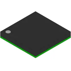
Las imágenes son solo para referencia
SC89171QDNR
- Fabricante
- Mfr. Parte #SC89171QDNR
- Paquete
- Hoja de datos
- En stock14382
100% original & Nuevo
24 horas listos para el envío
Garantía de 365 días
RFQ y Obtenga más descuentos
Especificaciones
| Manufacturer | JLCPCB Assembly |
| Package | QFN-24 (3.5x5.5x0.75) |
Descripción general
Description
This LDO can supply a specific output current while maintaining regulation under varying load conditions. It often includes protection features such as thermal shutdown and overcurrent protection, ensuring reliability and safety during operation.
The SC89171QDNR is available in a compact package, facilitating space-saving designs in consumer electronics, automotive, and industrial applications. Its performance characteristics, including fast transient response and low noise output, make it ideal for sensitive analog circuits.
For detailed specifications, including electrical characteristics and application circuits, consulting the manufacturer's datasheet is recommended.
Features
1. Input Voltage Range: Supports a wide input voltage range, typically up to 5.5V.
2. Output Voltage: Adjustable output voltage options, providing flexibility for various systems.
3. Low Dropout Voltage: Features low dropout voltage, ensuring stable output even with minimal input-output voltage differential.
4. High Output Current: Capable of delivering significant output current, suitable for powering demanding loads.
5. Low Quiescent Current: Designed for energy efficiency, minimizing power consumption during idle states.
6. Thermal Protection: Includes built-in thermal shutdown to prevent overheating.
7. Short-Circuit Protection: Offers short-circuit protection, enhancing reliability and safety.
8. Compact Package: Available in a small footprint package, ideal for space-constrained applications.
These features make the SC89171QDNR suitable for applications in consumer electronics, automotive, and industrial sectors, where efficient power management is critical.
Package
Pinout
1. Pin 1 (Offset Null): Used for offset voltage adjustment.
2. Pin 2 (Inverting Input, A): Inverting input for the first op-amp.
3. Pin 3 (Non-inverting Input, A): Non-inverting input for the first op-amp.
4. Pin 4 (Output, A): Output for the first op-amp.
5. Pin 5 (Supply Voltage, V- or GND): Negative power supply or ground.
6. Pin 6 (Output, B): Output for the second op-amp.
7. Pin 7 (Non-inverting Input, B): Non-inverting input for the second op-amp.
8. Pin 8 (Inverting Input, B): Inverting input for the second op-amp.
This configuration allows the device to be used in various analog signal processing applications.
Manufacturer
Application
Equivalent
Envío
Métodos de envíoNosotros
ofrecer servicios de envío globales a través de DHL, FedEx, TNT, UPS, o cualquier otro expediente de su elección.
Referencia de tarifas de envío (DHL/FedEx):
DHL: El costo de envío oscila entre $25-$45 (0.5kg), con un tiempo de entrega estimado de 2-5 días hábiles.
FedEx: El costo de envío oscila entre $25-$40 (0.5kg), con un tiempo de entrega estimado de 3-7 días hábiles.
UPS: El costo de envío oscila entre $25-$45 (0.5kg), con un tiempo de entrega estimado de 3-7 días hábiles.
TNT: El costo de envío oscila entre $25-$65 (0.5kg), con un tiempo de entrega estimado de 3-7 días hábiles.
EMS: El costo de envío oscila entre $30-$50 (0.5kg), con un plazo de entrega estimado de 7-15 días hábiles.
Correo aéreo registrado: El costo de envío es de $2-$4 (0.1kg), con un tiempo de entrega estimado de 5-20 días hábiles.
Pagos
Payment Methods
El plazo de pago es 100% prepagado.
Actualmente, solo aceptamos los siguientes métodos de pago:
1. de PayPal
2. Tarjeta de crédito/débito
3. Transferencia bancaria
Similar
-
![MX25V1635FZNQ03]() MX25V1635FZNQ03
Macronix
-
![MX29F400CBTI-70G]() MX29F400CBTI-70G
Macronix
-
![MX25V5126FM1I]() MX25V5126FM1I
Macronix
-
![MX25V2033FM1I]() MX25V2033FM1I
Macronix
-
![MX25V16066M1I02]() MX25V16066M1I02
Macronix
-
![MX30LF2G28AD-TI]() MX30LF2G28AD-TI
Macronix
-
![MX25R6435FBDIL0]() MX25R6435FBDIL0
Macronix
-
![MX25L25673GMI-10G]() MX25L25673GMI-10G
Macronix
-
![MX29GL512FHXFI-11G]() MX29GL512FHXFI-11..
Macronix
-
![MX25V1635FM2I]() MX25V1635FM2I
Macronix
-
![MX25U3232FZBI02]() MX25U3232FZBI02
Macronix
-
![MX25L6433FM2I-08G]() MX25L6433FM2I-08G
Macronix