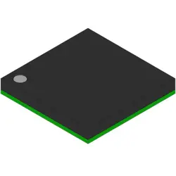
Las imágenes son solo para referencia
IS61WV51216BLL-10MLI
IC SRAM 8MBIT PARALLEL 48MINIBGA
- Fabricante
- Mfr. Parte #IS61WV51216BLL-10MLI
- Paquete 48-TFBGA
- Hoja de datos IS61WV51216BLL-10MLI DataSheet
- En stock4183
100% original & Nuevo
24 horas listos para el envío
Garantía de 365 días
RFQ y Obtenga más descuentos
Especificaciones
| Package | Tray |
| ProductStatus | Active |
| MemoryType | Volatile |
| MemoryFormat | SRAM |
| Technology | SRAM - Asynchronous |
| MemorySize | 8Mb (512K x 16) |
| MemoryInterface | Parallel |
| WriteCycleTime-WordPage | 10ns |
| AccessTime | 10 ns |
| Voltage-Supply | 2.4V ~ 3.6V |
| OperatingTemperature | -40°C ~ 85°C (TA) |
| MountingType | Surface Mount |
| Package/Case | 48-TFBGA |
Descripción general
Description
The device is organized as 32K words by 16 bits, and it supports both asynchronous read and write operations. It is available in multiple package options, including a 48-pin TSOP (Thin Small Outline Package), which facilitates easy integration into circuit boards. The IS61WV51216BLL-10MLI is ideal for use in networking, telecommunications, automotive, and industrial applications where reliability and speed are crucial.
Key features include low power consumption, enabling battery-operated devices, and a simple control interface, making it user-friendly for engineers.
Package
Pinout
### Pin Functions:
1. Address Inputs (A0-A18): 19 pins used to select the memory address.
2. Data Inputs/Outputs (DQ0-DQ15): 16 pins for data input and output.
3. Data Mask (DQML): 1 pin for data masking.
4. Bank Select (BA0, BA1): 2 pins to select the bank.
5. Chip Select (CS): 1 pin to enable or disable the device.
6. R/W (Read/Write): 1 pin to indicate the operation mode.
7. Clock (CLK): 1 pin for synchronization.
8. Clock Enable (CKE): 1 pin to enable or disable the clock.
9. Write Enable (WE): 1 pin to control write operations.
10. Output Enable (OE): 1 pin to control output.
11. Reset (RESET): 1 pin for resetting the device.
12. VDD/VSS: Power supply and ground pins.
This configuration allows for efficient data storage and retrieval in various applications.
Manufacturer
Application
Equivalent
1. MT18LSD51216 (Micron)
2. CY3S25610 (Cypress)
3. IDT71V516S (Integrated Device Technology)
4. K4S560832F (Samsung)
Always verify specifications for compatibility in your application.
Envío
Métodos de envíoNosotros
ofrecer servicios de envío globales a través de DHL, FedEx, TNT, UPS, o cualquier otro expediente de su elección.
Referencia de tarifas de envío (DHL/FedEx):
DHL: El costo de envío oscila entre $25-$45 (0.5kg), con un tiempo de entrega estimado de 2-5 días hábiles.
FedEx: El costo de envío oscila entre $25-$40 (0.5kg), con un tiempo de entrega estimado de 3-7 días hábiles.
UPS: El costo de envío oscila entre $25-$45 (0.5kg), con un tiempo de entrega estimado de 3-7 días hábiles.
TNT: El costo de envío oscila entre $25-$65 (0.5kg), con un tiempo de entrega estimado de 3-7 días hábiles.
EMS: El costo de envío oscila entre $30-$50 (0.5kg), con un plazo de entrega estimado de 7-15 días hábiles.
Correo aéreo registrado: El costo de envío es de $2-$4 (0.1kg), con un tiempo de entrega estimado de 5-20 días hábiles.
Pagos
Payment Methods
El plazo de pago es 100% prepagado.
Actualmente, solo aceptamos los siguientes métodos de pago:
1. de PayPal
2. Tarjeta de crédito/débito
3. Transferencia bancaria
Similar
-
![MX25L3233FM1I-08Q]() MX25L3233FM1I-08Q
Macronix
-
![MX25V1635FZNI]() MX25V1635FZNI
Macronix
-
![MX25V1635FZNQ03]() MX25V1635FZNQ03
Macronix
-
![MX66U1G45GXDI00]() MX66U1G45GXDI00
Macronix
-
![MX29GL512FHXFI-11G]() MX29GL512FHXFI-11..
Macronix
-
![MX25L2006EM1I-12G]() MX25L2006EM1I-12G
Macronix
-
![MX25L6433FM2I-08G]() MX25L6433FM2I-08G
Macronix
-
![MX25L12835FZ2I-10G]() MX25L12835FZ2I-10..
Macronix
-
![MX29LV160DTTI-70G]() MX29LV160DTTI-70G
Macronix
-
![MX29F040CTI-70G]() MX29F040CTI-70G
Macronix
-
![MX29F800CBTI-70G]() MX29F800CBTI-70G
Macronix
-
![MX25U51245GZ4I00]() MX25U51245GZ4I00
Macronix