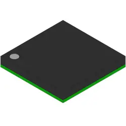
Las imágenes son solo para referencia
BUF16821AIPWPRQ1
IC AMP TFT-LCD 28HTSSOP
- Fabricante
- Mfr. Parte #BUF16821AIPWPRQ1
- Paquete 28-PowerTSSOP (0.173, 4.40mm Width)
- Hoja de datos
- En stock2828
100% original & Nuevo
24 horas listos para el envío
Garantía de 365 días
RFQ y Obtenga más descuentos
Especificaciones
| Supplier | Texas Instruments,Rochester Electronics, LLC |
| Package | Tape & Reel (TR),Cut Tape (CT),Bulk |
| Series | Automotive, AEC-Q100 |
| ProductStatus | Active |
| Applications | TFT-LCD Panels: Gamma Buffer, VCOM Driver |
| OutputType | Rail-to-Rail |
| NumberofCircuits | 18 |
| Current-Supply | 12 mA |
| Current-Output/Channel | 30 mA |
| Voltage-SupplySingle/Dual(±) | 9V ~ 20V |
| MountingType | Surface Mount |
| Package/Case | 28-PowerTSSOP (0.173, 4.40mm Width) |
Descripción general
Description
If you share the manufacturer or the datasheet, I’ll summarize concisely.
In general, a “BUF” device is a digital buffer/line driver used to fan out signals. A proper intro would cover:
- function and number of buffered channels
- supply voltage (Vcc) and input/output specs
- enable/tri-state control and timing
- packaging/revision (IPWPRQ1 indicates a specific package)
- typical applications (signal buffering, level shifting, bus interfacing)
- key performance metrics (propagation delay, power consumption)
Provide the manufacturer or a datasheet link, and I’ll draft a precise, under-200-word introduction.
Package
Pinout
Application
Envío
Métodos de envíoNosotros
ofrecer servicios de envío globales a través de DHL, FedEx, TNT, UPS, o cualquier otro expediente de su elección.
Referencia de tarifas de envío (DHL/FedEx):
DHL: El costo de envío oscila entre $25-$45 (0.5kg), con un tiempo de entrega estimado de 2-5 días hábiles.
FedEx: El costo de envío oscila entre $25-$40 (0.5kg), con un tiempo de entrega estimado de 3-7 días hábiles.
UPS: El costo de envío oscila entre $25-$45 (0.5kg), con un tiempo de entrega estimado de 3-7 días hábiles.
TNT: El costo de envío oscila entre $25-$65 (0.5kg), con un tiempo de entrega estimado de 3-7 días hábiles.
EMS: El costo de envío oscila entre $30-$50 (0.5kg), con un plazo de entrega estimado de 7-15 días hábiles.
Correo aéreo registrado: El costo de envío es de $2-$4 (0.1kg), con un tiempo de entrega estimado de 5-20 días hábiles.
Pagos
Payment Methods
El plazo de pago es 100% prepagado.
Actualmente, solo aceptamos los siguientes métodos de pago:
1. de PayPal
2. Tarjeta de crédito/débito
3. Transferencia bancaria
Similar
-
![MX25L3233FM1I-08Q]() MX25L3233FM1I-08Q
Macronix
-
![MX25V1635FZNI]() MX25V1635FZNI
Macronix
-
![MX25V1635FZNQ03]() MX25V1635FZNQ03
Macronix
-
![MX25V5126FM1I]() MX25V5126FM1I
Macronix
-
![MX25V4035FZUI]() MX25V4035FZUI
Macronix
-
![MX25V16066M2I02]() MX25V16066M2I02
Macronix
-
![MX25R6435FBDIL0]() MX25R6435FBDIL0
Macronix
-
![MX29GL512FHXFI-11G]() MX29GL512FHXFI-11..
Macronix
-
![MX25U25643GZNI00]() MX25U25643GZNI00
Macronix
-
![MX25R1635FZUIH0]() MX25R1635FZUIH0
Macronix
-
![MX25U3232FZBI02]() MX25U3232FZBI02
Macronix
-
![MX25U25645GXDI00]() MX25U25645GXDI00
Macronix