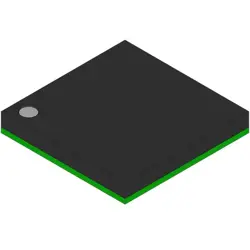
Las imágenes son solo para referencia
BSC190N15NS3 G
MOSFETs N-Ch 150V 50A TDSON-8 OptiMOS 3
- Fabricante
- Mfr. Parte #BSC190N15NS3 G
- Paquete
- Hoja de datos BSC190N15NS3 G DataSheet
- En stock25211
100% original & Nuevo
24 horas listos para el envío
Garantía de 365 días
RFQ y Obtenga más descuentos
Especificaciones
| Packaging | MouseReel |
| Standard Pack Qty | 5000 |
Descripción general
Description
Students can expect a mix of lectures, interactive discussions, and hands-on laboratory experiences, fostering an understanding of living organisms and their interactions with the environment. This course is essential for anyone interested in pursuing further studies in life sciences or related fields.
Features
1. Voltage Rating: It supports a maximum drain-to-source voltage (VDS) of 150V.
2. Current Rating: The continuous drain current (ID) is 190A, allowing for high current handling.
3. RDS(on): It offers a low on-resistance (RDS(on)) of approximately 0.015 ohms, enhancing efficiency and reducing power loss during operation.
4. Package Type: The device is typically available in a DPAK or similar package, facilitating easy mounting and thermal management.
5. Fast Switching Speed: It is designed for high-speed switching, making it suitable for applications like DC-DC converters, motor drives, and power inverters.
6. Thermal Performance: With a high maximum junction temperature rating, it provides reliable operation in demanding environments.
7. Gate Threshold Voltage: The gate threshold voltage (VGS(th)) ranges from 2 to 4V, enabling compatibility with low-voltage drive circuits.
Overall, the BSC190N15NS3 G is well-suited for high-efficiency power management solutions.
Package
Pinout
1. Gate (G) - This pin is used to control the MOSFET's switching state. A voltage applied to the gate creates an electric field that allows current to flow between the drain and source.
2. Drain (D) - This is the terminal through which the main current flows out of the device when it is in the 'on' state.
3. Source (S) - This pin is connected to the ground or negative voltage in typical applications, allowing current to flow from the drain to the source when the MOSFET is activated.
4. Body Diode (internal) - The device has an internal body diode that provides a path for current in the reverse direction, useful for inductive load applications.
For specific applications, the datasheet should be consulted for detailed electrical characteristics and ratings.
Manufacturer
Application
Equivalent
Envío
Métodos de envíoNosotros
ofrecer servicios de envío globales a través de DHL, FedEx, TNT, UPS, o cualquier otro expediente de su elección.
Referencia de tarifas de envío (DHL/FedEx):
DHL: El costo de envío oscila entre $25-$45 (0.5kg), con un tiempo de entrega estimado de 2-5 días hábiles.
FedEx: El costo de envío oscila entre $25-$40 (0.5kg), con un tiempo de entrega estimado de 3-7 días hábiles.
UPS: El costo de envío oscila entre $25-$45 (0.5kg), con un tiempo de entrega estimado de 3-7 días hábiles.
TNT: El costo de envío oscila entre $25-$65 (0.5kg), con un tiempo de entrega estimado de 3-7 días hábiles.
EMS: El costo de envío oscila entre $30-$50 (0.5kg), con un plazo de entrega estimado de 7-15 días hábiles.
Correo aéreo registrado: El costo de envío es de $2-$4 (0.1kg), con un tiempo de entrega estimado de 5-20 días hábiles.
Pagos
Payment Methods
El plazo de pago es 100% prepagado.
Actualmente, solo aceptamos los siguientes métodos de pago:
1. de PayPal
2. Tarjeta de crédito/débito
3. Transferencia bancaria
Similar
-
![MX25V1635FZNQ03]() MX25V1635FZNQ03
Macronix
-
![MX25V16066M1I02]() MX25V16066M1I02
Macronix
-
![MX30LF2G28AD-TI]() MX30LF2G28AD-TI
Macronix
-
![MX25L8035EM2I-10G]() MX25L8035EM2I-10G
Macronix
-
![MX29GL512FHXFI-11G]() MX29GL512FHXFI-11..
Macronix
-
![MX25U3232FZBI02]() MX25U3232FZBI02
Macronix
-
![MX25L12833FZNI-10G]() MX25L12833FZNI-10..
Macronix
-
![MX25U25645GXDI00]() MX25U25645GXDI00
Macronix
-
![MX29F040CQI-70G]() MX29F040CQI-70G
Macronix
-
![MX25L4006EM2I-12G]() MX25L4006EM2I-12G
Macronix
-
![MX25R4035FM1IL0]() MX25R4035FM1IL0
Macronix
-
![MX25L6473FM2I-08G]() MX25L6473FM2I-08G
Macronix