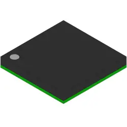
Las imágenes son solo para referencia
ADG819BRTZ
Analog Switch ICs SPDT (BBM)
- Fabricante
- Mfr. Parte #ADG819BRTZ
- Paquete
- Hoja de datos ADG819BRTZ DataSheet
- En stock21397
100% original & Nuevo
24 horas listos para el envío
Garantía de 365 días
RFQ y Obtenga más descuentos
Especificaciones
| Standard Pack Qty | 10000 |
Descripción general
Description
Key specifications include a low on-resistance (typically around 1.2Ω), which minimizes signal distortion and power loss, and fast switching speeds, providing efficient signal routing. The ADG819BRTZ is also characterized by low leakage current, enhancing its reliability in sensitive applications.
Its application areas include audio systems, data acquisition, and instrumentation, where signal integrity is crucial. The device is offered in a compact, surface-mount package, facilitating ease of integration into various electronic designs. Overall, the ADG819BRTZ is an ideal choice for engineers seeking reliable, low-power signal switching solutions.
Features
1. Low On-Resistance: Offers low on-resistance (typically 0.6 ohms at 5V) for minimal signal distortion.
2. Wide Voltage Range: Operates with a supply voltage range from 1.8V to 5.5V, making it suitable for various applications.
3. Fast Switching Speed: Provides quick switching with low propagation delay, ideal for high-speed data transmission.
4. Low Power Consumption: Consumes minimal power in the off state, enhancing battery life in portable devices.
5. TTL/CMOS Compatible: Compatible with both TTL and CMOS logic levels, facilitating integration into diverse circuits.
6. Break-Before-Make Switching: Prevents short circuits during switching operations, ensuring device safety.
7. Thermal Protection: Includes features to prevent overheating, enhancing reliability.
These attributes make the ADG819BRTZ suitable for applications in telecommunications, audio systems, and signal routing.
Package
Pinout
The primary functions of the pins are as follows:
1. Input/Output Pins (S1, S2, D1, D2): These pins serve as the signal paths for the switches. D1 and D2 are the common terminals, while S1 and S2 are the switched terminals.
2. Control Pins (IN1, IN2): These pins control the switch states. A high signal on IN1 or IN2 connects the respective switch to its output (D1 or D2).
3. Power Supply Pins (VDD, GND): VDD is the positive supply voltage pin, while GND is the ground reference pin.
4. NC (Not Connected): Pins designated as NC should not be connected to any external circuit.
The ADG819BRTZ is designed for low on-resistance and low distortion, making it suitable for various analog switching applications.
Manufacturer
Application
Equivalent
Envío
Métodos de envíoNosotros
ofrecer servicios de envío globales a través de DHL, FedEx, TNT, UPS, o cualquier otro expediente de su elección.
Referencia de tarifas de envío (DHL/FedEx):
DHL: El costo de envío oscila entre $25-$45 (0.5kg), con un tiempo de entrega estimado de 2-5 días hábiles.
FedEx: El costo de envío oscila entre $25-$40 (0.5kg), con un tiempo de entrega estimado de 3-7 días hábiles.
UPS: El costo de envío oscila entre $25-$45 (0.5kg), con un tiempo de entrega estimado de 3-7 días hábiles.
TNT: El costo de envío oscila entre $25-$65 (0.5kg), con un tiempo de entrega estimado de 3-7 días hábiles.
EMS: El costo de envío oscila entre $30-$50 (0.5kg), con un plazo de entrega estimado de 7-15 días hábiles.
Correo aéreo registrado: El costo de envío es de $2-$4 (0.1kg), con un tiempo de entrega estimado de 5-20 días hábiles.
Pagos
Payment Methods
El plazo de pago es 100% prepagado.
Actualmente, solo aceptamos los siguientes métodos de pago:
1. de PayPal
2. Tarjeta de crédito/débito
3. Transferencia bancaria
Similar
-
![MX25L3233FZBI-08Q]() MX25L3233FZBI-08Q
Macronix
-
![MX25V1635FZNI]() MX25V1635FZNI
Macronix
-
![MX25V5126FM1I]() MX25V5126FM1I
Macronix
-
![MX25V16066M2I02]() MX25V16066M2I02
Macronix
-
![MX25L25673GMI-08G]() MX25L25673GMI-08G
Macronix
-
![MX29GL512FHXFI-11G]() MX29GL512FHXFI-11..
Macronix
-
![MX25U25643GZNI00]() MX25U25643GZNI00
Macronix
-
![MX25U3232FZBI02]() MX25U3232FZBI02
Macronix
-
![MX25U6435FM2I-10G]() MX25U6435FM2I-10G
Macronix
-
![MX25U25645GXDI00]() MX25U25645GXDI00
Macronix
-
![MX25L25645GXDI-08G]() MX25L25645GXDI-08..
Macronix
-
![MX29LV640ETTI-70G]() MX29LV640ETTI-70G
Macronix