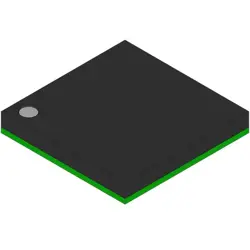
Las imágenes son solo para referencia
AD8556ACPZ
ADI Pgm Sensor Amp W/EMI Filters
- Fabricante
- Mfr. Parte #AD8556ACPZ
- Paquete
- Hoja de datos
- En stock7333
100% original & Nuevo
24 horas listos para el envío
Garantía de 365 días
RFQ y Obtenga más descuentos
Especificaciones
| Packaging | Reel |
| Standard Pack Qty | 1500 |
Descripción general
Description
Key specifications include a typical offset voltage of 50µV, a high open-loop gain of 120 dB, and a wide bandwidth, with a gain-bandwidth product of 1 MHz. The amplifier also offers rail-to-rail output, enabling it to drive loads close to the supply rails.
The AD8556 is commonly used in applications such as sensor signal conditioning, data acquisition systems, and portable instrumentation, where precision and low power consumption are critical. Its small package size (LFCSP) and low quiescent current further enhance its utility in compact electronic designs.
Features
- Supply Voltage Range: Operates from a single supply of 2.7V to 12V or dual supplies of ±1.35V to ±6V.
- Low Power Consumption: Typically consumes only 1.1 mA per amplifier.
- Low Offset Voltage: Offers a maximum input offset voltage of 50 µV, ensuring high accuracy.
- Rail-to-Rail Output: Provides output that can swing very close to the supply rails, maximizing dynamic range.
- Wide Bandwidth: Features a gain-bandwidth product of 1.2 MHz, making it suitable for a range of frequencies.
- High Slew Rate: Provides a slew rate of 0.5 V/µs, allowing for fast signal changes.
- Temperature Range: Operates over a temperature range of -40°C to +125°C, suitable for industrial applications.
- Package: Available in a 8-lead LFCSP package, optimizing for space-saving designs.
These attributes make the AD8556ACPZ ideal for precision signal processing in instrumentation, sensor conditioning, and other applications requiring low noise and low drift.
Package
Pinout
Pin Count and Functions:
1. Pin 1 (Offset Null): Used for offset voltage adjustment.
2. Pin 2 (Inverting Input, -): The input terminal for the inverting signal.
3. Pin 3 (Non-Inverting Input, +): The input terminal for the non-inverting signal.
4. Pin 4 (V- or Ground): Negative power supply or ground connection.
5. Pin 5 (Output): The output terminal where the amplified signal is provided.
6. Pin 6 (V+ or Positive Supply): Positive power supply connection.
7. Pin 7 (Offset Null): Used for offset voltage adjustment.
8. Pin 8 (NC): No connection; not used.
This device is suitable for various applications requiring low offset voltage, low noise, and high precision.
Manufacturer
Application
Equivalent
Envío
Métodos de envíoNosotros
ofrecer servicios de envío globales a través de DHL, FedEx, TNT, UPS, o cualquier otro expediente de su elección.
Referencia de tarifas de envío (DHL/FedEx):
DHL: El costo de envío oscila entre $25-$45 (0.5kg), con un tiempo de entrega estimado de 2-5 días hábiles.
FedEx: El costo de envío oscila entre $25-$40 (0.5kg), con un tiempo de entrega estimado de 3-7 días hábiles.
UPS: El costo de envío oscila entre $25-$45 (0.5kg), con un tiempo de entrega estimado de 3-7 días hábiles.
TNT: El costo de envío oscila entre $25-$65 (0.5kg), con un tiempo de entrega estimado de 3-7 días hábiles.
EMS: El costo de envío oscila entre $30-$50 (0.5kg), con un plazo de entrega estimado de 7-15 días hábiles.
Correo aéreo registrado: El costo de envío es de $2-$4 (0.1kg), con un tiempo de entrega estimado de 5-20 días hábiles.
Pagos
Payment Methods
El plazo de pago es 100% prepagado.
Actualmente, solo aceptamos los siguientes métodos de pago:
1. de PayPal
2. Tarjeta de crédito/débito
3. Transferencia bancaria
Similar
-
![MX25V1635FZNI]() MX25V1635FZNI
Macronix
-
![MX25V5126FM1I]() MX25V5126FM1I
Macronix
-
![MX25V2033FM1I]() MX25V2033FM1I
Macronix
-
![MX25L8035EM2I-10G]() MX25L8035EM2I-10G
Macronix
-
![MX25L25673GMI-08G]() MX25L25673GMI-08G
Macronix
-
![MX25L25673GMI-10G]() MX25L25673GMI-10G
Macronix
-
![MX29GL512FHXFI-11G]() MX29GL512FHXFI-11..
Macronix
-
![MX25U51279GXDR00]() MX25U51279GXDR00
Macronix
-
![MX25U25643GZNI00]() MX25U25643GZNI00
Macronix
-
![MX25R1635FZUIH0]() MX25R1635FZUIH0
Macronix
-
![MX25L12833FZ2I-10G]() MX25L12833FZ2I-10..
Macronix
-
![MX25L25645GXDI-08G]() MX25L25645GXDI-08..
Macronix