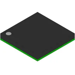
Las imágenes son solo para referencia
10CX105YF672I5G
IC FPGA 236 I/O 672FBGA
- Fabricante
- Mfr. Parte #10CX105YF672I5G
- Paquete FBGA-672
- Hoja de datos
- En stock2961
100% original & Nuevo
24 horas listos para el envío
Garantía de 365 días
RFQ y Obtenga más descuentos
Especificaciones
| Package | Tray |
| Series | Cyclone® 10 GX |
| ProductStatus | Active |
| NumberofLABs/CLBs | 38000 |
| NumberofLogicElements/Cells | 104000 |
| TotalRAMBits | 8641536 |
| NumberofI/O | 236 |
| Voltage-Supply | 0.9V |
| MountingType | Surface Mount |
| OperatingTemperature | -40°C ~ 100°C (TJ) |
| Package/Case | 672-BBGA, FCBGA |
Descripción general
Description
The "YF" designation indicates a specific package type, while "672" refers to the number of I/O pins. The "I5G" suffix usually denotes the temperature range and other specific configurations. Cyclone 10 devices are known for their ease of integration, versatile I/O options, and support for various interfaces, including LVDS and SERDES.
Overall, the 10CX105YF672I5G is ideal for developers looking to implement custom logic solutions with a balance of performance and efficiency.
Features
1. Logic Elements: Approximately 105K logic elements, providing ample resources for complex designs.
2. Memory: Integrated memory blocks including up to 4 Mbits of embedded memory, enabling efficient data storage and processing.
3. I/O Pins: Supports up to 672 user I/O pins, allowing for extensive interfacing capabilities.
4. Power Efficiency: Designed for low power consumption, making it suitable for portable and battery-operated applications.
5. Performance: Offers high performance with up to 200 MHz operation frequency, suitable for a variety of applications.
6. Protocol Support: Supports various communication protocols including LVDS, PCIe, and others, facilitating connectivity.
7. Development Tool Compatibility: Compatible with the Intel Quartus Prime development software for ease of design and testing.
This FPGA is widely used in applications such as industrial automation, automotive systems, and communications.
Package
Pinout
The primary functions of these pins include:
1. I/O Pins: For general-purpose input/output operations.
2. Power Supply Pins: To provide various voltage levels required for the FPGA's operation.
3. Configuration Pins: Used for programming the device and loading configuration data.
4. Clock Pins: For external clock sources to synchronize operations.
5. Dedicated Functionality Pins: These may include pins for specific protocols like JTAG, PLL, or other application-specific signals.
For detailed pin configuration and functionalities, it's recommended to consult the datasheet or technical documentation provided by Intel.
Manufacturer
Application
Equivalent
1. Intel Cyclone V (e.g., 5CEFA2F23C7N)
2. Xilinx Artix-7 (e.g., XC7A100T)
3. Lattice ECP5 (e.g., LFE5U-85F)
4. Microsemi SmartFusion2 (e.g., M2S050)
These alternatives offer similar performance and functionality, suitable for similar applications in digital design.
Envío
Métodos de envíoNosotros
ofrecer servicios de envío globales a través de DHL, FedEx, TNT, UPS, o cualquier otro expediente de su elección.
Referencia de tarifas de envío (DHL/FedEx):
DHL: El costo de envío oscila entre $25-$45 (0.5kg), con un tiempo de entrega estimado de 2-5 días hábiles.
FedEx: El costo de envío oscila entre $25-$40 (0.5kg), con un tiempo de entrega estimado de 3-7 días hábiles.
UPS: El costo de envío oscila entre $25-$45 (0.5kg), con un tiempo de entrega estimado de 3-7 días hábiles.
TNT: El costo de envío oscila entre $25-$65 (0.5kg), con un tiempo de entrega estimado de 3-7 días hábiles.
EMS: El costo de envío oscila entre $30-$50 (0.5kg), con un plazo de entrega estimado de 7-15 días hábiles.
Correo aéreo registrado: El costo de envío es de $2-$4 (0.1kg), con un tiempo de entrega estimado de 5-20 días hábiles.
Pagos
Payment Methods
El plazo de pago es 100% prepagado.
Actualmente, solo aceptamos los siguientes métodos de pago:
1. de PayPal
2. Tarjeta de crédito/débito
3. Transferencia bancaria
Similar
-
![MX25R8035FM1IL0]() MX25R8035FM1IL0
Macronix
-
![MX25L3233FM1I-08Q]() MX25L3233FM1I-08Q
Macronix
-
![MX25V1635FZNI]() MX25V1635FZNI
Macronix
-
![MX66U1G45GXDI00]() MX66U1G45GXDI00
Macronix
-
![MX25V5126FM1I]() MX25V5126FM1I
Macronix
-
![MX25L8035EM2I-10G]() MX25L8035EM2I-10G
Macronix
-
![MX29GL512FHXFI-11G]() MX29GL512FHXFI-11..
Macronix
-
![MX25L2006EM1I-12G]() MX25L2006EM1I-12G
Macronix
-
![MX25V1635FM2I]() MX25V1635FM2I
Macronix
-
![MX25L12833FZNI-10G]() MX25L12833FZNI-10..
Macronix
-
![MX25U25645GXDI00]() MX25U25645GXDI00
Macronix
-
![MX29LV640ETTI-70G]() MX29LV640ETTI-70G
Macronix